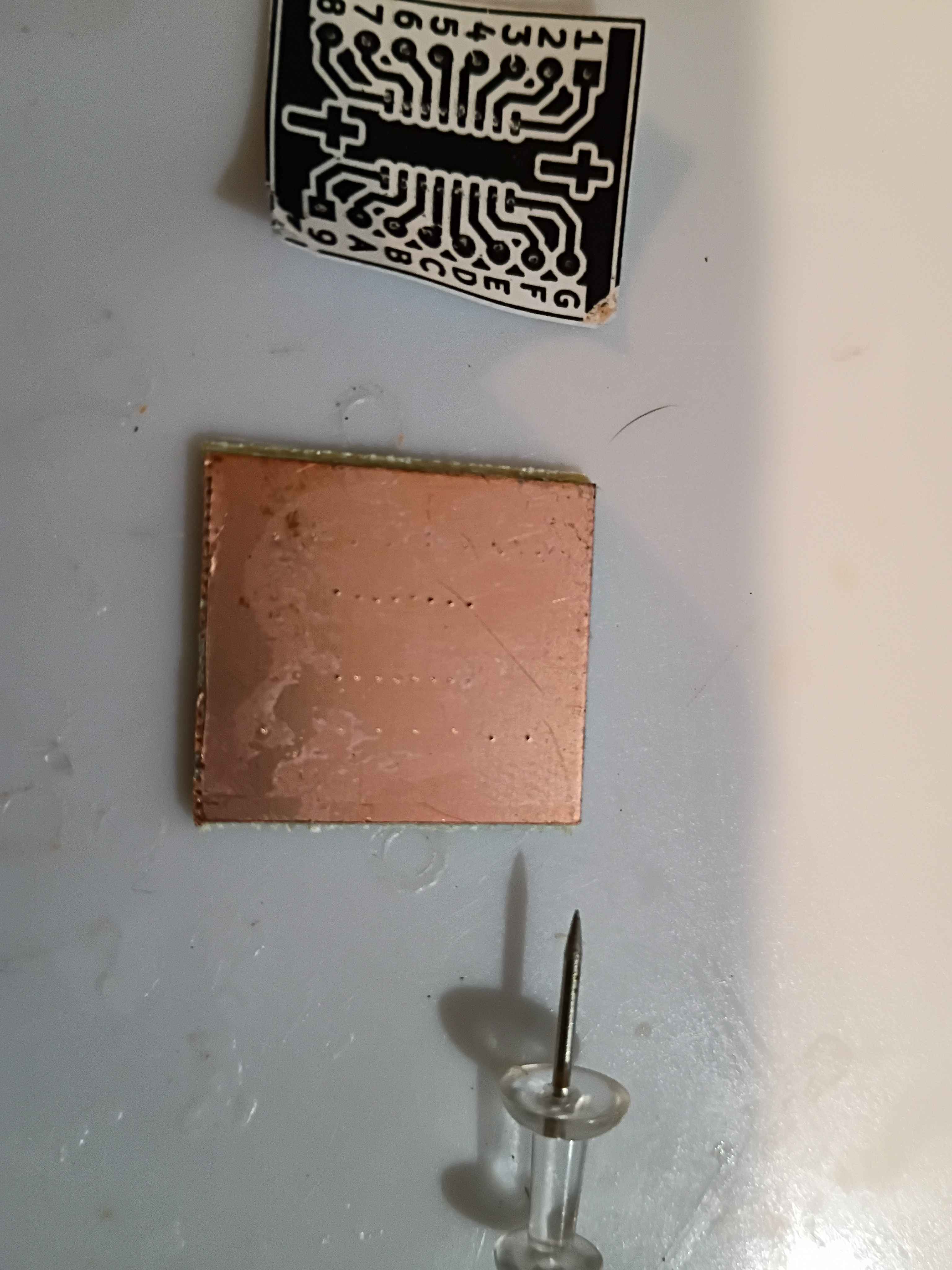
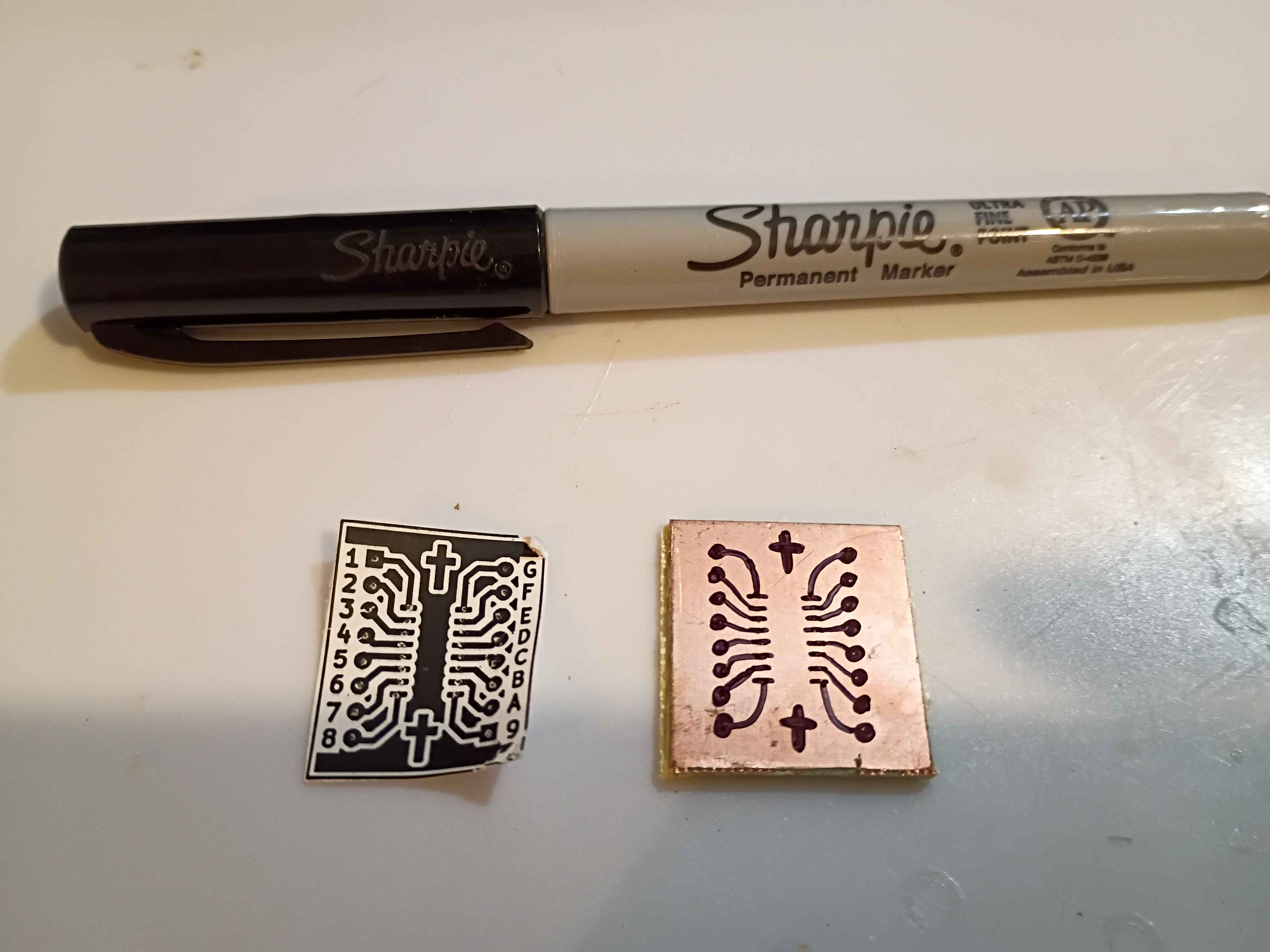
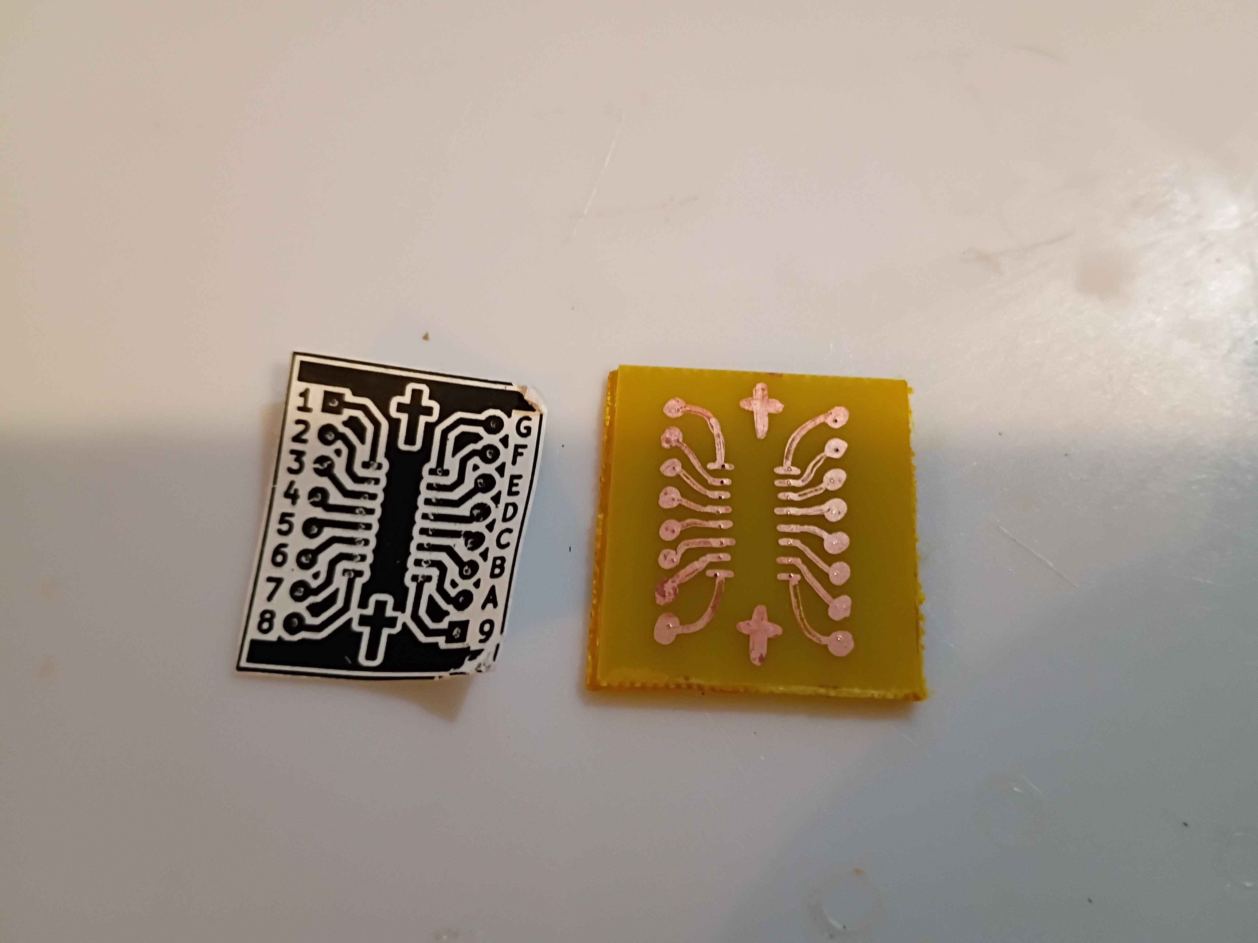
Successfully attempted a new artisanal PCB design transfer method for in-house etching. It involves adhering a non-mirrored image of the traces to the copper face of the copper clad board and pressing in the center of all pads (and corners of all trace line segments) with a thumb tack. Then the paper is removed and the pads and traces are reconstructed by hand using an ultra-fine point sharpie. This has been shown to resist Ferric Chloride etching solution in a previous study. The first attempt was a resounding success, and only took 30 minutes from start to etched board with a very low probability of failure. If the traces are marked incorrectly, they can be wiped away with acetone and easily redrawn.