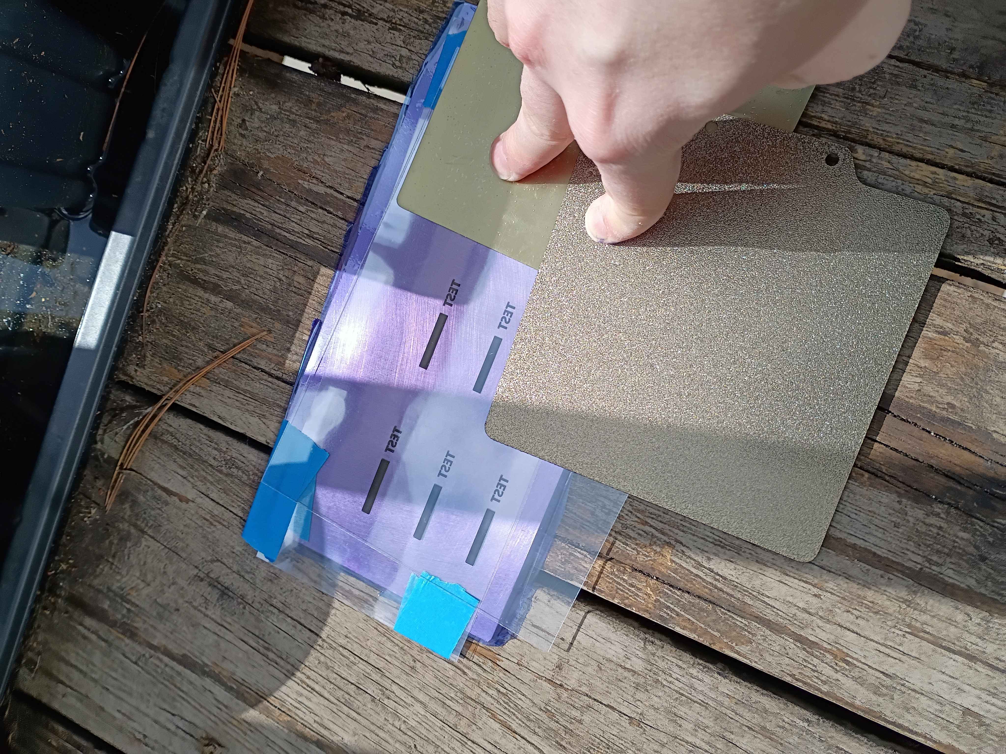
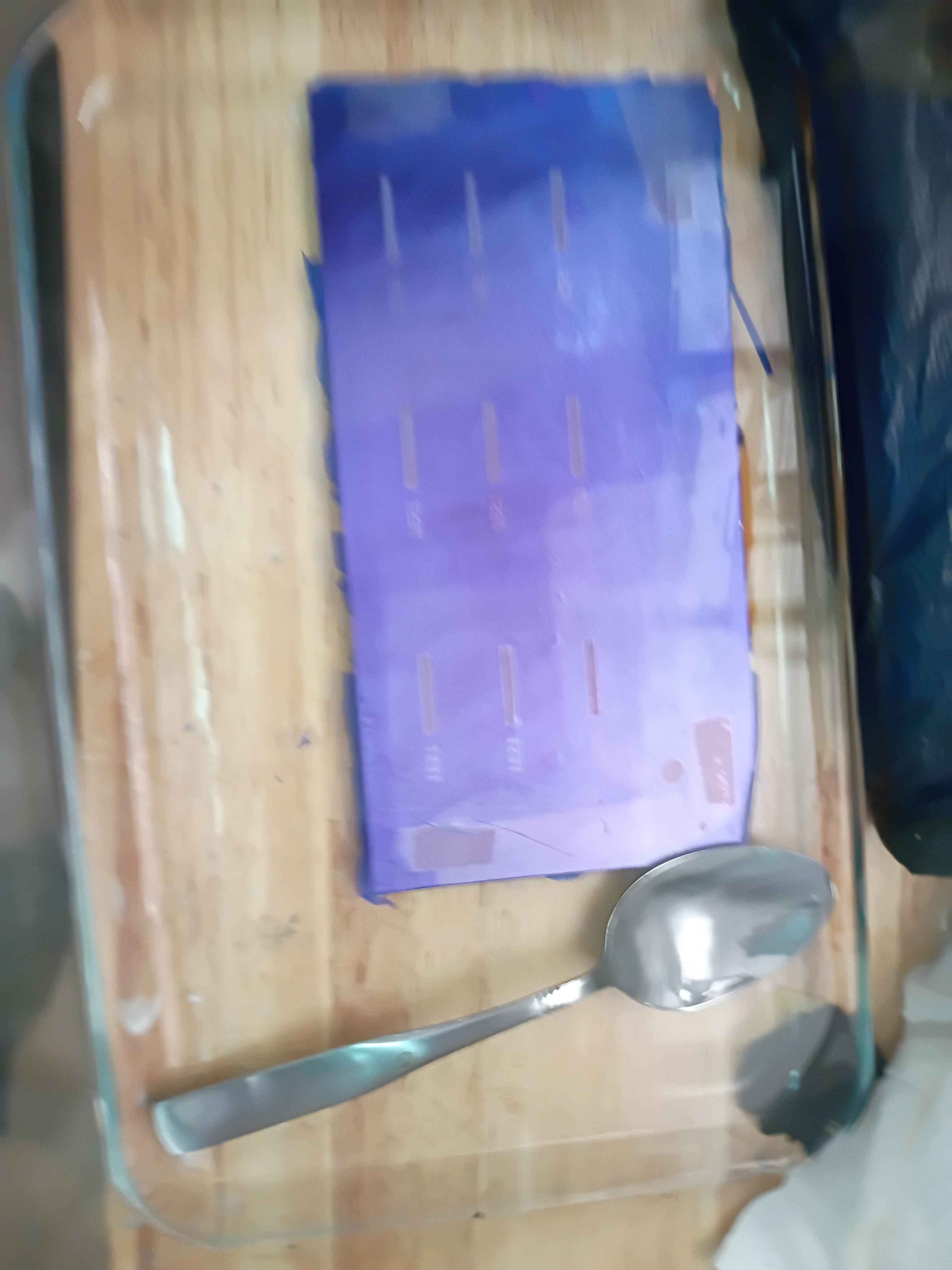
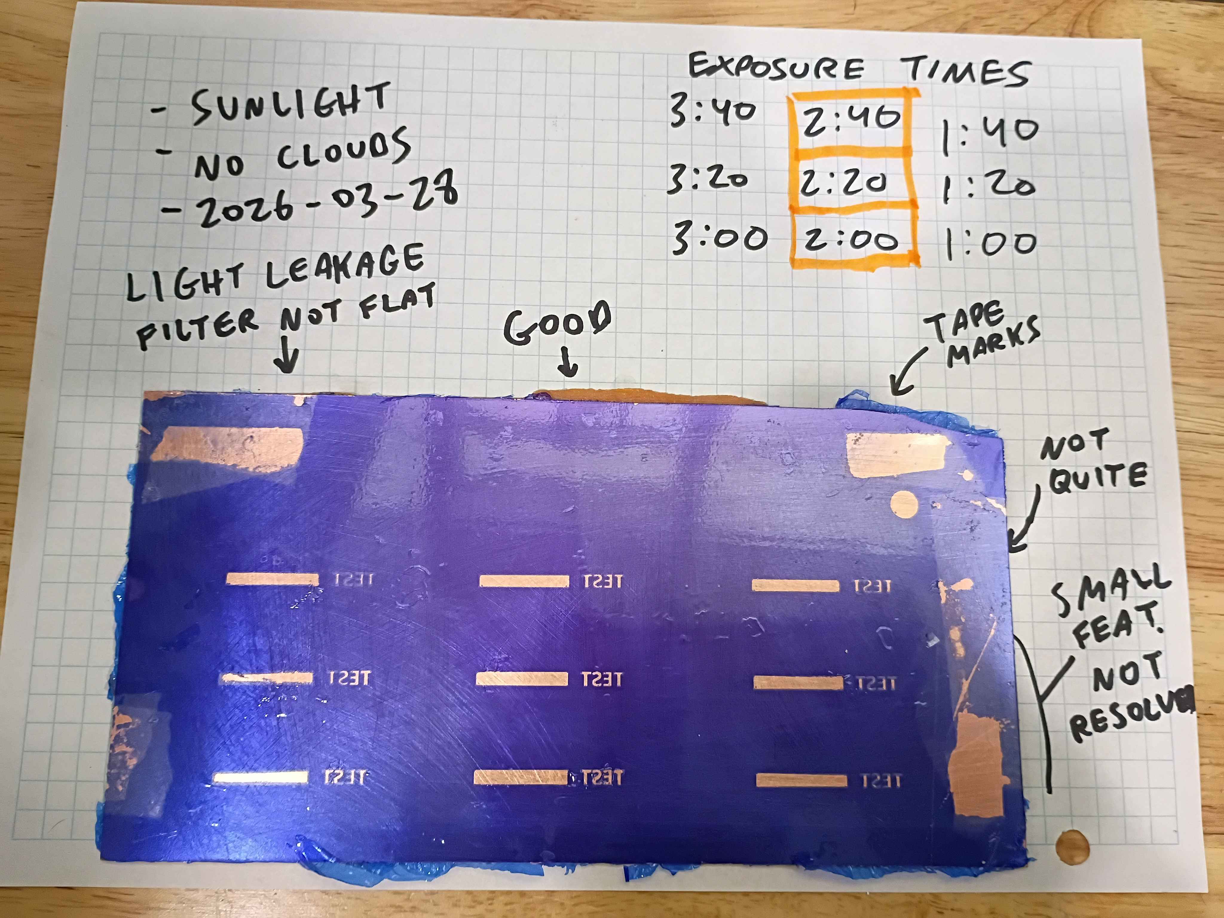
Re-attempted the use of dry film photoresist for mask transfer onto copper clad boards. Board was scuffed with 500 grit and then cleaned with acetone and IPA (actually I messed up the first film transfer and removed the failed attempt with acetone and wiped clean with IPA). The film was affixed mostly mechanically, with bubbles being removed by sliding them out by finger pressure. Limited heat was used, iron on low seemed not to help very much, though research suggests it helps the bond. A double layer of a light filter laser-printed on transparency sheets was taped to the surface and regions were exposed to the sun on this cloudless day in Bridgeport, CT (2026-03-28) for between 1:00 and 3:40 minutes. The filters were held flat to the surface by a thin acrylic sheet. After developing in 1L tap water with 1 tbsp dissolved washing soda for several minutes, the board was wiped dry. All the exposures >1 minute appear passable, though because the light filters were not pressed flat the entire time, the longer exposure times seem to have experienced some light leakage, though that could likely be avoided with a better clamping setup. Qualitatively the 2:20 exposure time looks best, with the 0.4mm features in the text being well defined. This is more than enough fidelity for most circuit traces and IC package pin spacing. Exposures below 2:00 also seem reasonable though the edges are not well resolved. I think this is because the photoresist is not sufficiently cured along the edges. The conclusion is that this method of transferring a copper mask with relatively fine features can be used successfully without even a UV cure station. It would appear able to resolve smaller features with a greater degree of success than toner transfer. If I were to use this in the future, I would recommend clamping a thick glass panel on the outer surface to keep the light filters pressed flat and cure for roughly 2:30.